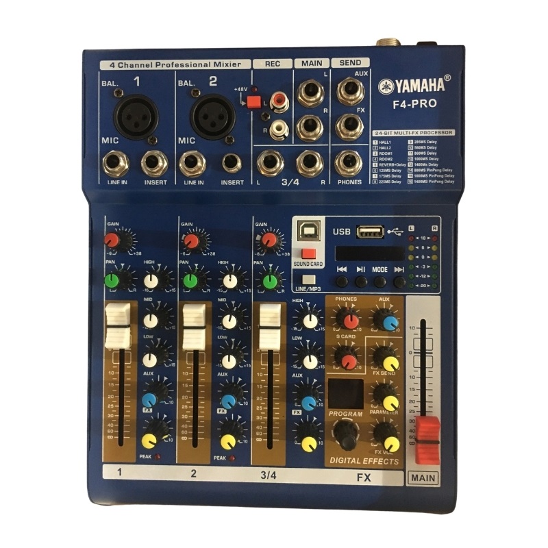
Bàn Mixer F4 Pro
950000
The JDM-040 motherboard powers mid-generation PlayStation 4 Slim and Pro controllers (DualShock 4). Finding an accurate JDM-040 schematic diagram is essential for fixing common issues like stick drift, power failures, and unล่าสุด button responses.
PlayStation 4 DualShock 4 controller (CUH-ZCT2 model series)
Sony has never released official schematics for any DualShock 4 revision to the public. Unlike open‑source hardware or some vintage consoles, the DS4’s circuitry is treated as proprietary information. As a result, repair guides and troubleshooting discussions rely entirely on reverse‑engineered diagrams, high‑resolution PCB scans, and the collective knowledge of the modding community.
The charging port and bottom EXT port are managed by a separate daughterboard (FPC), but the main JDM-040 board houses the primary logic for battery regulation. 2. Power Management and Charging Battery Voltage: Standard 3.7V Li-ion, typically 1000mAh. jdm040 schematic exclusive
Stick drift is the most common hardware failure on the JDM-040. The controller uses 10k-ohm Alps potentiometers. Each analog stick consists of two independent potentiometers: one for the X-axis (horizontal) and one for the Y-axis (vertical).
JDM-040 Schematic Exclusive: Ultimate Guide to the PS4 Slim Controller Board
A complete schematic for the JDM-040 highlights the complex interaction between the main processor (MCU), button matrix, analog sticks, and power management ICs. Key Functional Areas Unlike open‑source hardware or some vintage consoles, the
The JDM‑040 is a later revision of the DualShock 4 mainboard. It is commonly found in PS4 controllers with the model number and is distinguished by a blue light bar on the touchpad (earlier revisions used a different light guide). The corresponding small charging‑port board is labelled JDS‑040 (sometimes printed as JDS‑040 or JDM‑040 on the flex cable).
Connected directly to the filtered 3.2V system rail.
I cannot produce a meaningful essay on the specific phrase because, to the best of my knowledge, no verified or widely recognized electronic schematic, product, or technical standard exists under that exact name. to the best of my knowledge
Earlier PS4s used 4+1 phase VRMs. The JDM-040 exclusive schematic shows a controller, but phase 5 and 6 are cloned via a secondary gate driver. This means 90% of "APU failure" repairs are actually a dead phase #5 filter capacitor. The schematic gives you the exact part number (SP-Cap 560uF, 2.5V) and its alternate location hidden under the EMI shield.
It controlled drones.
: Traces for the main button inputs move to the upper right side of the PCB front layer . This makes soldering custom macro paddles or rapid-fire chips significantly easier.
The JDM-040 motherboard powers mid-generation PlayStation 4 Slim and Pro controllers (DualShock 4). Finding an accurate JDM-040 schematic diagram is essential for fixing common issues like stick drift, power failures, and unล่าสุด button responses.
PlayStation 4 DualShock 4 controller (CUH-ZCT2 model series)
Sony has never released official schematics for any DualShock 4 revision to the public. Unlike open‑source hardware or some vintage consoles, the DS4’s circuitry is treated as proprietary information. As a result, repair guides and troubleshooting discussions rely entirely on reverse‑engineered diagrams, high‑resolution PCB scans, and the collective knowledge of the modding community.
The charging port and bottom EXT port are managed by a separate daughterboard (FPC), but the main JDM-040 board houses the primary logic for battery regulation. 2. Power Management and Charging Battery Voltage: Standard 3.7V Li-ion, typically 1000mAh.
Stick drift is the most common hardware failure on the JDM-040. The controller uses 10k-ohm Alps potentiometers. Each analog stick consists of two independent potentiometers: one for the X-axis (horizontal) and one for the Y-axis (vertical).
JDM-040 Schematic Exclusive: Ultimate Guide to the PS4 Slim Controller Board
A complete schematic for the JDM-040 highlights the complex interaction between the main processor (MCU), button matrix, analog sticks, and power management ICs. Key Functional Areas
The JDM‑040 is a later revision of the DualShock 4 mainboard. It is commonly found in PS4 controllers with the model number and is distinguished by a blue light bar on the touchpad (earlier revisions used a different light guide). The corresponding small charging‑port board is labelled JDS‑040 (sometimes printed as JDS‑040 or JDM‑040 on the flex cable).
Connected directly to the filtered 3.2V system rail.
I cannot produce a meaningful essay on the specific phrase because, to the best of my knowledge, no verified or widely recognized electronic schematic, product, or technical standard exists under that exact name.
Earlier PS4s used 4+1 phase VRMs. The JDM-040 exclusive schematic shows a controller, but phase 5 and 6 are cloned via a secondary gate driver. This means 90% of "APU failure" repairs are actually a dead phase #5 filter capacitor. The schematic gives you the exact part number (SP-Cap 560uF, 2.5V) and its alternate location hidden under the EMI shield.
It controlled drones.
: Traces for the main button inputs move to the upper right side of the PCB front layer . This makes soldering custom macro paddles or rapid-fire chips significantly easier.
HỆ THỐNG CỬA HÀNG
Cơ sở 2
Giờ làm việc: Vui lòng gọi điện trước khi đến.
Xem bản đồCơ sở 3
Giờ làm việc: Vui lòng gọi điện trước khi đến.
Xem bản đồCơ sở 4
Giờ làm việc: Vui lòng gọi điện trước khi đến.
Xem bản đồThông tin
Chính sách chung
Hỗ trợ khách hàng
Phương thức thanh toán
Kết nối với chúng tôi